Skip to content
1.Development Trends of On-Board Chargers (OBC) for Electric Vehicles
China’s new energy vehicle (NEV) market has experienced rapid growth, with annual sales reaching 6.887 million units in 2022 (a 93.4% year-on-year increase), capturing 26% market share. According to the China Association of Automobile Manufacturers (CAAM), NEV sales are projected to exceed 9 million units in 2023, growing by 35% with a 32.6% market penetration rate.
This sustained expansion drives surging demand for On-Board Chargers (OBC), as virtually every electric vehicle requires one. In 2022, OBC installations soared to 5.1287 million units (77.6% YoY growth), with the market expected to reach RMB 30 billion in 2023, reflecting immense potential.
Technical Role of OBCs:
When charging via AC charging piles (Figure 1), the OBC—installed within the vehicle—serves as the core energy conversion component. It enables:
Autonomous command execution to complete charging cycles
Safe, automated full charging of traction batteries
Dynamic adjustment of current/voltage parameters based on Battery Management System (BMS) data
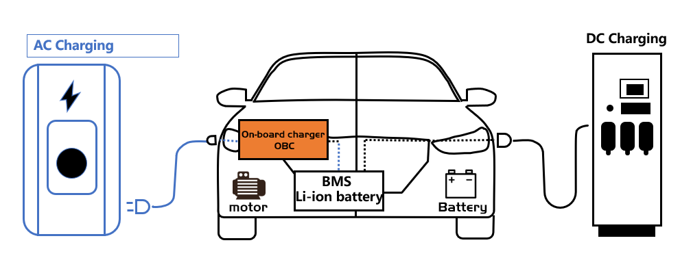
Figure 1: Electric Vehicle Charging Methods
To meet spatial constraints and safety requirements, On-Board Chargers (OBCs) must achieve stringent standards in:
- Power density
- Charging efficiency
- Weight/volume
- Output voltage/current range
- Safety and reliability
Addressing user and OEM demands has driven OBCs through critical challenges:
- High Power Density: Requires high-frequency/high-efficiency circuit topologies and optimized structural design.
- Bidirectional Energy Flow: Enables powering AC devices via BMS, necessitating bidirectional topologies.
- Compact High-Power Design: Drives OBCs toward intelligent and highly integrated solutions.
Tripartite Technological Evolution:
| Component | Advancement Direction |
|---|---|
| Charging Piles | High-power, high-voltage, bidirectional, wide-range |
| Batteries | Higher voltage (400V → 800V), increased power |
| OBCs | High-power, multi-functional integration, new materials |
OBCs are now evolving toward bidirectional charging/discharging, intelligent control, and system integration. Current mainstream OBC configurations are summarized in Table 1.
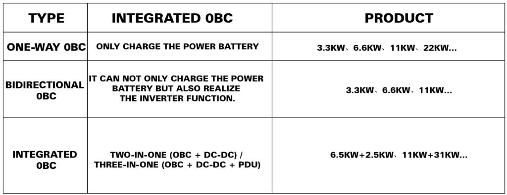
From a power perspective, 3.3 kW and 6.6 kW products currently dominate the market. Regarding output voltage, OBC solutions from companies like BYD Fudi Power and VMAX already support 800V platforms. Furthermore, amid intensifying industry competition, silicon carbide (SiC) power devices are being adopted in domestically produced OBCs. Leading firms including VMAX, Inpower, and Shinry Technologies have unveiled SiC-based OBC solutions.
2.On-Board Charger (OBC) Circuit Structure
The On-Board Charger (OBC) generally employs a two-stage architecture (as shown in Figure 2). The front-stage PFC (Power Factor Correction) circuit is primarily responsible for power factor correction and typically outputs 400V DC. The rear-stage DC/DC circuit draws power from the PFC bus, providing isolation and voltage regulation functions. Since the load connected to the DC/DC converter is the battery, which generally requires a high-voltage DC output of 200-500V, the rear stage must utilize a high-efficiency, wide-range isolated DC/DC topology.
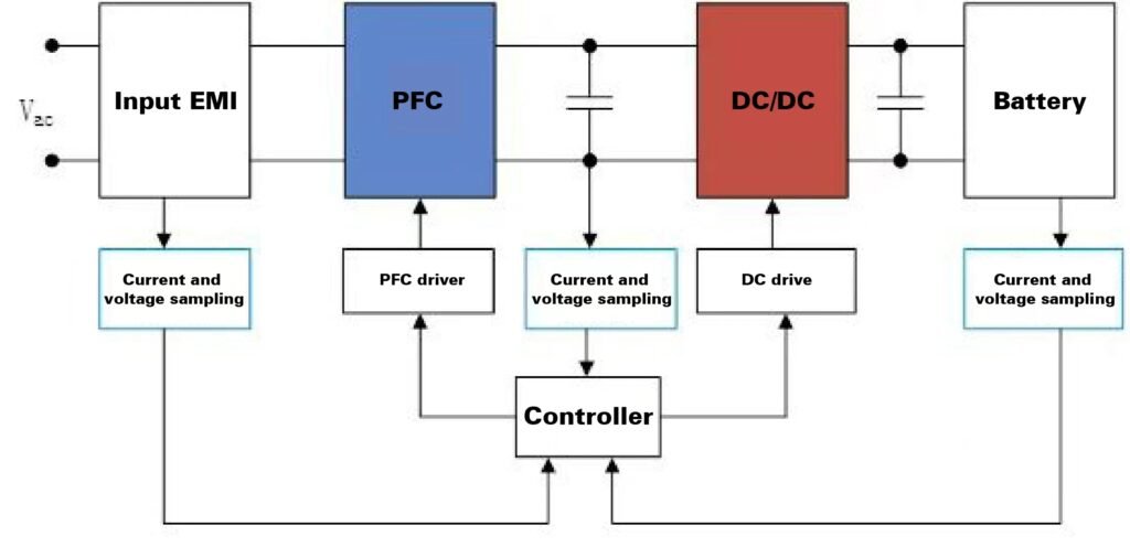
Figure 2: Two-Stage OBC Topology
2.1 Single-Stage PFC Circuit
Common PFC Circuit Topologies
The Boost converter topology is widely used in PFC circuits, including:
- Conventional Bridged Boost PFC
- Interleaved Parallel Boost PFC
- Bridgeless Boost PFC
- Dual Bridgeless Boost PFC
- Totem-Pole Boost PFC
(1) Conventional Bridged Boost PFC (Figure 3):
- When Q1 is ON:
- Positive half-cycle conduction path: D1 → L1 → Q1 → D4
- Negative half-cycle conduction path: D2 → L1 → Q1 → D3
- When Q1 is OFF:
- Positive half-cycle conduction path: D1 → L1 → D5 → Rd → D4
- Negative half-cycle conduction path: D2 → L1 → D5 → Rd → D3
In all operational states, three switching devices conduct simultaneously.
Advantages: Simple circuit topology and straightforward control.
Disadvantages: Only one switching device (Q1) bears the full voltage/current stress, resulting in excessive voltage and current stress that makes this topology unsuitable for high-power applications.
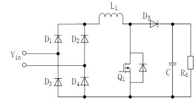
Figure 3: Conventional Bridged Boost PFC
(2) Interleaved Parallel Boost PFC (Figure 4):
This topology consists of two identical Boost PFC converters connected in parallel. Key characteristics include:
Disadvantage: Requires increased component count (additional switching devices)
Reduced PFC inductor size
180° phase-shifted control of the two inductor currents
→ Minimizes input/output current ripple
→ Allows downsizing of EMI filters
Maintains identical power flow direction and control logic to conventional bridged Boost PFC
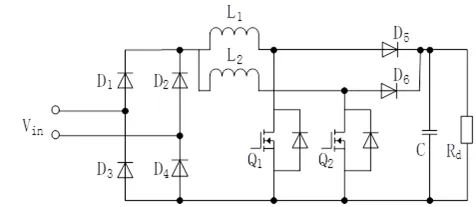
Figure 4: Interleaved Parallel Boost PFC
(3) Bridgeless Boost PFC (Figure 5):
This topology eliminates the rectifier bridge from conventional bridged PFC, reducing component count. Operational details:
- Positive Half-Cycle:
- Q1 OFF: Conduction path: L1 → D1 → Rd → Q2 → L2
- Q1 ON: Conduction path: L1 → Q1 → Q2 → L2
- Negative Half-Cycle:
- Q2 OFF: Conduction path: L2 → D2 → Rd → Q1 → L1
- Q2 ON: Conduction path: L2 → Q2 → Q1 → L1
Advantages vs. Conventional Bridged PFC:
- Fewer conducting switching devices → Higher system efficiency
- Simplified control (Q1/Q2 share identical gate-drive signals when switches have built-in anti-parallel diodes)
Critical Limitations:
Coupled common-mode noise requiring isolation
Current sensing complexity
Floating DC output terminals → Induces severe EMI issues due to:
Unreferenced (“floating”) ground connection

Figure 5: Bridgeless Boost PFC
(4) Dual Bridgeless Boost PFC (Figure 6):
This topology improves EMI performance compared to standard bridgeless PFC. Operational paths:
- Positive Half-Cycle:
- Q1 OFF: Conduction path: L1 → D1 → Rd → D4
- Q1 ON: Conduction path: L1 → Q1 → D4
- Negative Half-Cycle:
- Q2 OFF: Conduction path: L2 → D2 → Rd → D3
- Q2 ON: Conduction path: L2 → Q2 → D3
Key Characteristics:
Trade-off: Increased system cost due to additional components
Control scheme identical to basic bridgeless PFC
Added diodes (D3/D4) suppress EMI significantly
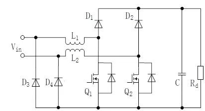
Figure 6: Dual Bridgeless Boost PFC
(5) Totem-Pole Boost PFC (Figure 7):
This topology resolves EMI issues inherent in bridgeless PFC. Operational paths:
- Positive Half-Cycle:
- *Q1 OFF / Q2 ON:* Conduction path: L → Q2 → D2
- *Q2 OFF / Q1 ON:* Conduction path: L → Q1 → Rd → D2
- Negative Half-Cycle:
- *Q1 OFF / Q2 ON:* Conduction path: D1 → Rd → Q2 → L
- *Q1 ON / Q2 OFF:* Conduction path: D1 → Q1 → L
Critical Challenges:
Elevated system cost
Control complexity
Floating gate-drive requirement for high-side switches → Increases design difficulty
Reverse recovery issues in Q1/Q2 → Significantly increases switching losses
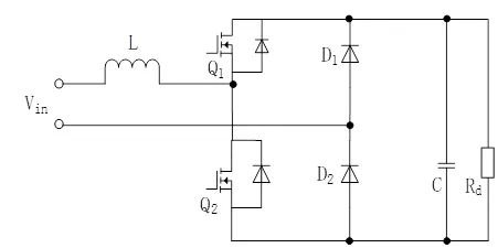
Figure 7: Totem-Pole Boost PFC
2.2 Secondary-Stage DC/DC Converter
Isolated DC/DC converter topologies (e.g., Phase-Shifted Full-Bridge, Dual Active Bridge, LLC Resonant Circuit) are preferred for OBC applications due to their power handling capacity and electrical safety compliance. Common isolated topologies include:
(1) Phase-Shifted Full-Bridge Circuit (Figure 8):
- Delivers wide-range voltage output (down to zero voltage)
- Gate-drive phase control:
- Q1/Q3 (leading leg): 180° phase difference
- Q2/Q4 (lagging legs): Phase-lagged relative to Q1/Q3
- Soft-switching achievement:
Resonant operation between transformer leakage inductance and switch junction capacitance enables Zero-Voltage Switching (ZVS).
Critical Limitations:
Bulky LC output filter → Increases size and power losses
Duty cycle loss at secondary side due to leakage inductance
Voltage spikes across secondary diodes
Figure 8: Phase-Shifted Full-Bridge Circuit
(2) Dual Active Bridge (DAB) Circuit (Figure 9):
This topology controls power flow direction and magnitude through phase shift modulation between primary and secondary H-bridges. Key features include:
- Achieves Zero-Voltage Switching (ZVS)
- Bidirectional power transfer capability
- High power density (>3 kW/L) and peak efficiency (>98%)
- Dominant solution for high-power bidirectional DC/DC conversion
Primary Applications:
Electric vehicle charging systems
Aerospace power distribution
Energy storage integration
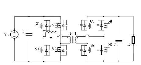
Figure 9: Dual Active Bridge (DAB) Circuit
(3) LLC Resonant Circuit (Figure 10):
This topology achieves soft-switching operation with wide voltage regulation range across a narrow frequency variation. Key advantages include:
High efficiency (typ. >98%) and low EMI noise
Superior load transient performance
Magnetic integration: Transformer leakage inductance reused as magnetizing inductance
Reduces magnetic component size
Increases power density (>5 W/cm³)
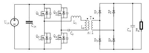
Figure 10: LLC Resonant Circuit
3.Leakage Protection Requirements for On-Board Chargers (OBC)
The increasing complexity of OBC circuit topologies—driven by advanced charging/discharging demands—elevates risks of leakage faults and complicates leakage current waveforms. Traditional Type AC/A residual current devices (RCDs) can only detect AC or pulsating DC leakage currents, failing to protect against complex OBC-generated currents (e.g., DC components). Therefore, Type B RCDs must be employed to monitor leakage currents during OBC operation. Type B RCDs detect:
- Sinusoidal AC signals
- Pulsating DC currents
- Smooth DC currents
making them the optimal safety solution for EVs, OBCs, and charging stations.
Critical Standard Reference:
Per QC/T 895-2011 “Conductive On-Board Chargers for Electric Vehicles”* (Figure: Control Pilot Circuit):
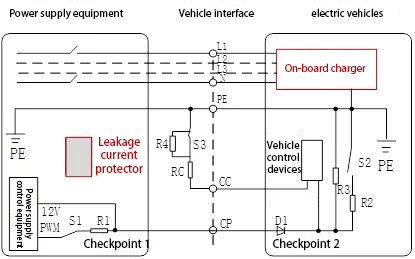
Figure 11: On-Board Charger (OBC) Input Control Pilot Circuit Diagram
MAGTRON utilizes its independently developed iFluxgate® chip technology, capable of detecting complex leakage current components—including both AC and DC currents. As a Type B residual current device (RCD), it outperforms traditional leakage protectors with superior reliability, sensitivity, and safety. This technology has been widely applied across multiple sectors such as charging piles and photovoltaic inverters (as shown in Figure 12), establishing an industry benchmark.
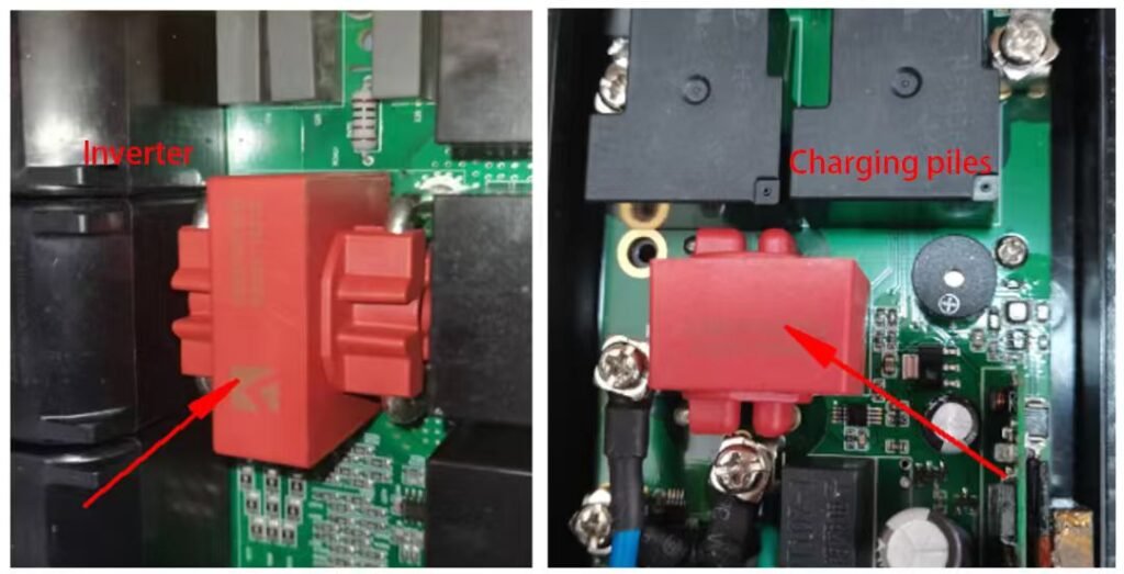
Figure 12: MAGTRON Product Applications
References:
[1] Xu, H. (2018). Development and Optimization of On-Board Charger Based on New National Standards for Electric Vehicles [Master’s thesis, East China University of Technology].
[2] Xu, X. K. (2018). *Design of 3.3kW On-Board Charger and Analysis of EMI Issues* [Master’s thesis, Nanjing University of Aeronautics and Astronautics]. DOI:10.27239/d.cnki.gnhhu.2018.000291.
[3] Dai, H. C. (2020). Circuit and Control System Design for Electric Vehicle On-Board Charger (OBC) [Master’s thesis, Zhejiang University]. DOI:10.27461/d.cnki.gzjdx.2020.000729.
[4] Fan, G. (2021). Research on High-Efficiency High-Power-Density DC/DC Converter for On-Board Chargers [Master’s thesis, Zhejiang University]. DOI:10.27461/d.cnki.gzjdx.2021.000244.
[5] QC/T 895-2011. Conductive On-Board Charger for Electric Vehicles.